- 您现在的位置:买卖IC网 > Sheet目录983 > HI5805EVAL1 (Intersil)EVALUATION PLATFORM HI5805
�� �
�
�Application� Note� 9707�
�Reference� Generator,� V� ROUT� and� V� RIN�
�The� HI5805� has� an� internal� reference� voltage� generator,�
�therefore� no� external� reference� voltage� is� required.� V� ROUT�
�must� be� connected� to� V� RIN� when� using� the� internal�
�reference.� Internal� to� the� converter,� two� reference� voltages�
�of� 1.3V� and� 3.3V� are� generated� making� for� a� fully� differential�
�analog� input� signal� range� of� ±� 2V.�
�The� HI5805� can� be� used� with� an� external� reference.� The�
�converter� requires� only� one� external� reference� voltage�
�The� difference� between� the� converter's� two� internally�
�generated� voltage� references� is� 2V.� For� the� AC� coupled�
�differential� input,� (Figure� 3),� if� V� IN� is� a� 2V� P-P� sinewave� with� -�
�V� IN� being� 180� degrees� out� of� phase� with� V� IN� ,� the� converter�
�will� be� at� positive� full� scale� when� the� V� IN+� input� is� at� V� DC� +� 1V�
�and� the� V� IN-� input� is� at� V� DC� -� 1V� (V� IN+� -� V� IN-� =� +2V).�
�Conversely,� the� ADC� will� be� at� negative� full� scale� when� the�
�V� IN+� input� is� equal� to� V� DC� -� 1V� and� V� IN-� is� at� V� DC� +� 1V� (V� IN+�
�-� V� IN-� =� -2V).�
�connected� to� the� V� RIN� pin� with� V� ROUT� left� open.� The�
�evaluation� board� is� configured� with� V� ROUT� connected� to� V� RIN�
�through� a� 0� ?� resistor,� R� 15� .� If� it� is� desired� to� evaluate� the�
�+5V�
�V� IN� +�
�2.0V� P-P�
�V� IN� -�
�VDC� =� 4.0V�
�+5V�
�performance� of� the� converter� utilizing� an� externally� provided�
�reference� voltage,� R� 15� can� be� removed� and� the� alternate�
�reference� voltage� can� be� brought� in� through� twisted� pair� wire� or�
�coaxial� cable.� The� latter� would� be� the� recommended� method�
�since� it� would� provide� the� greatest� immunity� to� externally�
�coupled� noise� voltages.� In� order� to� minimize� overall� converter�
�noise� it� is� recommended� that� adequate� high� frequency�
�decoupling� be� provided� at� the� reference� input� pin,� V� RIN� .�
�0V�
�V� IN� +�
�V� IN� +�
�2.0V� P-P�
�2.0V� P-P�
�V� IN� -�
�1.0V� <� VDC� <� 4.0V�
�V� IN� -�
�VDC� =� 1.0V�
�0V�
�Analog� Input�
�The� fully� differential� analog� input� of� the� HI5805� A/D� can� be�
�con?gured� in� various� ways� depending� on� the� signal� source�
�and� the� required� level� of� performance.�
�Differential� Analog� Input� Con?guration�
�A� fully� differential� connection� (Figure� 3)� will� yield� the� best�
�performance� from� the� HI5805� A/D� converter.� Since� the�
�HI5805� is� powered� off� a� single� +5V� supply,� the� analog� input�
�must� be� biased� so� it� lies� within� the� analog� input� common�
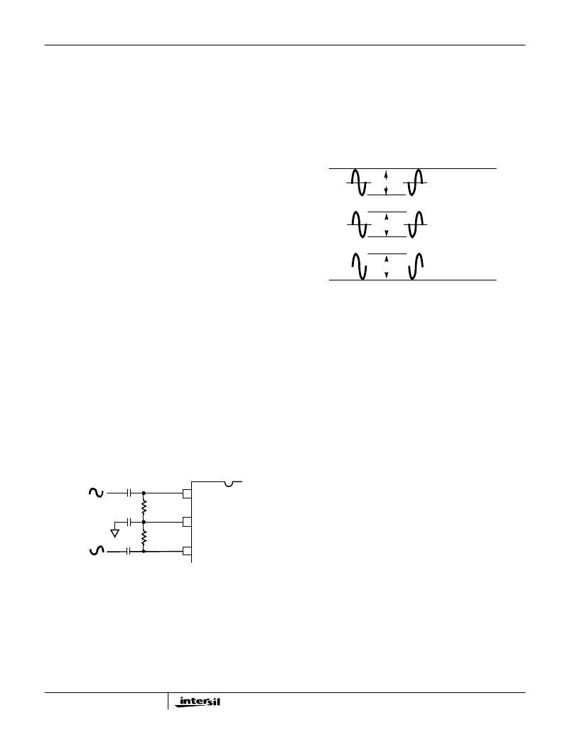
�mode� voltage� range� of� 1.0V� to� 4.0V.� Figure� 4� illustrates� the�
�differential� analog� input� common� mode� voltage� range� that�
�the� converter� will� accommodate.� The� performance� of� the�
�ADC� does� not� change� signi?cantly� with� the� value� of� the�
�common� mode� voltage.�
�FIGURE� 4.� DIFFERENTIAL� ANALOG� INPUT� COMMON� MODE�
�VOLTAGE� RANGE�
�Evaluation� Board� Layout� and� Power� Supplies�
�The� HI5805� evaluation� board� is� a� four� layer� board� with� a� layout�
�optimized� for� the� best� performance� of� the� ADC.� This� application�
�note� includes� an� electrical� schematic� of� the� evaluation� board,� a�
�component� parts� list,� a� component� placement� layout� drawing�
�and� reproductions� of� the� various� board� layers� used� in� the� board�
�stack-up.� The� user� should� feel� free� to� copy� the� layout� in� their�
�application.� Refer� to� the� component� layout� and� the� evaluation�
�board� electrical� schematic� for� the� following� discussions.�
�The� HI5805� monolithic� A/D� converter� has� been� designed�
�with� separate� analog� and� digital� supply� and� ground� pins� to�
�keep� digital� noise� out� of� the� analog� signal� path.� The�
�evaluation� board� provides� separate� low� impedance� analog�
�and� digital� ground� planes� on� layer� 2.� Since� the� analog� and�
�V� IN�
�-V� IN�
�V� IN� +�
�V� DC�
�V� IN� -�
�HI5805�
�digital� ground� planes� are� connected� together� at� a� single�
�point� where� the� power� supplies� enter� the� board,� DO� NOT� tie�
�them� together� back� at� the� power� supplies.�
�The� analog� and� digital� supplies� are� also� kept� separate� on�
�the� evaluation� board� and� should� be� driven� by� clean� linear�
�regulated� supplies.� The� external� power� supplies� can� be�
�hooked� up� with� wires� to� the� plated� through� holes� marked�
�FIGURE� 3.� AC� COUPLED� DIFFERENTIAL� INPUT�
�A� 2.3V� DC� bias� voltage� source,� VDC,� half� way� between� the� top�
�and� bottom� internally� generated� reference� voltages,� is� made�
�available� to� the� user� to� help� simplify� circuit� design� when� using� a�
�differential� input.� This� low� output� impedance� voltage� source� is�
�not� designed� to� be� a� reference� but� makes� an� excellent� bias�
�source� and� stays� within� the� analog� input� common� mode�
�voltage� range� over� temperature.� The� DC� voltage� source� has� a�
�temperature� coefficient� of� about� +200ppm/� o� C.�
�3-4�
�+5VAIN,� +5VAIN1,� -5VAIN,� +5VDIN,� +5VD1IN,� +5VD2IN,�
�-5VDIN,� AGND� and� DGND� near� the� analog� prototyping� area.�
�+5VDIN,� +5VD1IN,� +5VD2IN� and� -5VDIN� are� digital�
�supplies� and� should� be� returned� to� DGND.� +5VAIN,�
�+5VAIN1� and� -5VAIN� are� the� analog� supplies� and� should� be�
�returned� to� AGND.� Table� 1� lists� the� operational� supply�
�voltages,� typical� current� consumption� and� the� evaluation�
�board� circuit� function� being� powered.� Single� supply�
�operation� of� the� converter� is� possible� but� the� overall�
�performance� of� the� converter� may� degrade.�
�发布紧急采购,3分钟左右您将得到回复。
相关PDF资料
HI5828EVAL2
EVALUATION PLATFORM HI5828
HI5960SOICEVAL1
EVALUATION PLATFORM SOIC HI5960
HI7188EVAL
EVALUATION PLATFORM HI7188
HI7190EVAL
EVALUATION PLATFORM HI7190
HJ4-L-DC12V
RELAY GEN PURPOSE 4PDT 5A 12V
HL2-HP-AC100V-F
RELAY GEN PURPOSE DPDT 10A 100V
HLM01510Z16K50JJ
RES 16.5K OHM 15W 5% WW
HMC1043-DEMO
DEMONSTRATION BOARD FOR HMC1043
相关代理商/技术参数
HI5806IB
制造商:Rochester Electronics LLC 功能描述:- Bulk
HI5808
制造商:INTERSIL 制造商全称:Intersil Corporation 功能描述:12-Bit, 9MSPS A/D Converter
HI5808_01
制造商:INTERSIL 制造商全称:Intersil Corporation 功能描述:12-Bit, 9MSPS A/D Converter
HI5808BIB
制造商:INTERSIL 制造商全称:Intersil Corporation 功能描述:12-Bit, 9MSPS A/D Converter
HI5808BIBR4499
制造商:Rochester Electronics LLC 功能描述:- Bulk 制造商:Harris Corporation 功能描述:
HI5808BIBS2503
制造商:Rochester Electronics LLC 功能描述:- Bulk
HI5808EVAL1
制造商:INTERSIL 制造商全称:Intersil Corporation 功能描述:12-Bit, 10 MSPS A/D Converter
HI5810
制造商:INTERSIL 制造商全称:Intersil Corporation 功能描述:CMOS 10 Microsecond, 12-Bit, Sampling A/D Converter with Internal Track and Hold